

Specimen support for SEM, SIMS, AFM.
These may be used for mounting very fine particulate matter. They are chemically inert and make good substrates for growing or mounting cells.
They are also useful when this smooth, inert background is required and for the determination of resolution and contrast of "in-the-lens" SEMs equipped with high brightness electron emitters. Additionally, conducting specimens, or non-conducting specimens in low vacuum or low voltage SEM, may be viewed without coating.
Si chips are opaque, have low electrical resistance, are very smooth, brittle and hard like glass. Si chips are chemically quite inert. These chips are pre-cleaned, but for tissue and cell culture, additional cleaning and sterilising may be required.
Unlike glass, Si chips are crystalline and they are cut on the >111< orientation.
The wafers are cut into chips measuring 5 x 5mm, 5 x 7mm or 10 x 10mm.
Properties
Orientation (111)
Resistance 1-30 Ohms
Type P (Boron) if 1 primary flat Type N (Phosphor) if also a secondary flat, 45 degrees from primary flat, is present
No SiO2 top coating
Wafer thickness is 460 - 530µm
Wafer is polished on one side
After dicing they are rinsed in DI water for cleaning
Peters, K.R., Working at higher magnifications in scanning electron microscopy with secondary and backscattered electrons on metal coated biological specimens and imaging macromolecular cell membrane structures, 1985 Scanning Electron Microscopy, 1985, IV, 159.
Apkarian, R.P., High-resolution signal detection of specimen-specific secondary electrons in an analytical SEM, "Proc.. 44th Ann. Meeting of the EMSA", 1986, G.W. Bailey, Ed., San Francisco Press, 658.
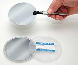
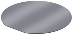
These 2", 3", 4" and 6" diameter silicon wafers can be used either as a substrate for thin film research or to make small silicon substrates by dicing the wafer into smaller pieces using a scriberand the Wafer Cleaving / Glass Breaking Pliers. The wafer is shipped in a wafer carrier.
Properties:
- Orientation: <111> or <100> for 6" wafer
- Resistance: 1-30 Ohms
- Type P: (Boron) (1 primary flat)
- No SiO2 top coating
- Wafer thickness:
- ⌀2" = 9 - 13 mill (230-330µm)
- ⌀3" = 13.6 - 18.5 mill (345-470µm)
- ⌀4" = 18.7 - 22.6 mill (475-575µm)
- ⌀6" = 23.6 - 25.2 mill (600-690µm)
- Roughness: 2nm
- TTV: = <20µm
- Wafer is polished on one side

The Ultra-Flat SiO2 substrates consist of a 200nm thermally grown amorphous SiO2 film on an ultra-flat silicon wafer. SiO2 is one of the most characterized materials and is widely used in semiconductor manufacturing, thin film research and as substrate for growing cells. It can be directly used as substrate for AFM and SEM imaging. The ultra-flat thermal silicon dioxide substrates are available in 6" wafer and conveniently diced 5x5mm, 5x7mm and 10x10mm chips. The 6" wafer is shipped in a 6" wafer carrier, the diced pieces are shipped in a Gel-Pak box. The special clean dicing process involves coating the wafer with photo resist before dicing and removing it after dicing which produces debris-free SiO2 substratres. All products are packed in class 10 clean room conditions.
Properties for thermal SiO2 substrates:
- Orientation: <100>
- Grade: Prime / CZ Virgin
- Resistance: 1-50 Ohm/cm
- Type: P / Dopant: Boron
- Wafer Thickness: 655-695 µm
- TTV: <= 7µm / STIR: <= 1.0µm
- Warp: <=40µm / Bow: <= 40µm
- Particles: <=20@>= 3.0µm
- Front surface: Polished
- Back Surface: Etched
- Flat: 1 per SEMI Standard (flat length 57.5+/12.5mm)
- Film: 200nm +/- 5% Thermal Oxide (SiO2), amorphous
- Size: 6" (150mm) diameter wafer or 5x5mm, 5x7mm or 10x10mm diced chips
- Roughness: Typical 2-3 Å
Ultra-Flat 6" diameter silicon wafer for demanding substrate studies. Can also be used as substrate for AFM or SEM samples by dicing the wafer into smaller pieces using a scriber and the Wafer Cleaving / Glass Breaking Pliers. The 6" ultra-flat silicon wafer is shipped in a 6" wafer carrier.
Properties for 6" (150mm)ultra-flat wafer:
- Orientation: <100>
- Grade: Prime / CZ Virgin
- Resistivity: 1-10 Ohm/cm
- Type: P / Dopant: Boron
- Wafer Thickness: 675 +/- 25µm
- TTV: <= 1.5µm
- Warp: <=30µm / Bow: <= 30µm
Particles: <= 30@>=0.2µm - Front surface: Polished
- Back Surface: Etched
- Flat: 1 per SEMI Standard (flat length 57.5 ±2.5mm)
- Roughness: Typical 2-3 Å