SEM or LM
100 markings with divisions of 0.01mm, on a nickel-plated copper disc.
Used for low-mag checks of an SEM or, unmounted, for light microscopy.
Documents
The CDMS Critical Dimensions and Magnification Standard is made on an ultra flat silicon substrate with a precise 50µm chromium deposition for the features up to 5µm and a combination of 50µm gold over 20µm chromium for the features sizes from 2µm to 100µm. The Cr and Au/Cr on Si provides excellent contrast both in SE and BSE imaging mode. The features are easier to determine than on etched Si standards. Since the silicon substrate, the chromium and the chromium/gold features are all conductive there are no charging issues with this calibration standard. Due to its sturdy construction the CDMS standard can be cleaned using a plasma cleaner.
The smaller features are nested for easy navigation and quick calibration. The accuracy of the features is 0.3% or better. The actual size of the standard is 2.5 x 2.5mm with a thickness of 625µm ±25µm. There is no coating on the Si surface. Each CDMS calibration standard has a unique identification number.
CDMS-1T is fully traceable with features from 2.0mm to 1µm for a magnification range from 10x - 20,000x; ideal for desk top SEMs and low to medium magnification applications.
TEM & STEM
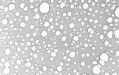
This film has numerous holes of varying sizes and is suitable for adjusting astigmatism and during alignment of the TEM. Mounted on a 3mm copper grid.

TEM
This test specimen is made on a holey carbon film which has been shadowed with gold and a coating of graphitised carbon particles. Particles protruding over the edge of a hole are best for testing high resolution performance. The evaporated gold forms small poly-crystalline islands and within these islands lattice fringes can be resolved. This specimen is also used to measure contamination rates in the electron microscope by noting the deposition rate of carbon within the holes of the gold film.
Documents
For EM magnification calibration
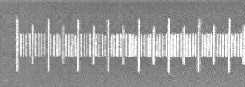
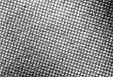
These are replicas of high-precision diffraction gratings and they are highly suited to the magnification calibration of electron microscopes. They are mounted on 200 mesh, 3mm copper grids. The grating is made by a grating instrument, which rules lines at equal intervals. Single lines never deviate from the nominal interval by 4%, but over a number of ruled lines these gratings, for all practical applications are absolutely correct. It is prudent to choose a grating that will include, within a photograph, at least several lines; use lower line numbers for lower magnifications with a TEM, and with the lesser magnifying SEMs.
Instructions are included with the grating and they are also given in our User Notes below. It must be appreciated that an instrument calibration is useful only for a given accelerating current and when similar lens currents are used. The objective lens, in particular, should be set to the calibrated setting, and the specimen initially brought into focus by using the Z control. TEM grids should always be inserted with the specimen down to achieve similar working distance. The down orientation is preferable especially when the specimen is on a support film.
SEM & very low power TEM
Germanium shadowed carbon replica of a ruled (lines, not waffles) diffraction grating having 600 lines/mm (15,240 lines/"). Actual grating spacing is 1667 nm. Mounted on a 200 mesh copper grid.
Documents
For TEM and & high power SEM
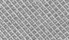
Cross ruled (waffle), 2160 lines/mm (54864 lines/"), carbon replica.
Documents
For low power TEM & SEM
As above but 28,800 lines per inch, with actual grating spacings of 882 nm.

The nominal value of the effective camera length of an EM operating in the selected area mode is not sufficiently accurate for calculations of lattice spacing. The actual value of camera length must be calibrated at the same accelerating voltage and objective lens setting by reference to a known substance with well defined diffraction spacings. A normal specimen is evaporated film of aluminium. Very small crystallite size yields ring patterns suitable for calibration. The specimen is supplied with a list of the principal lattice spacings. Made on a G400, 400 square mesh copper Gilder grid.
Documents
When changing from a selected area image of a specimen to a diffraction pattern, the strength of the intermediate lens is changed, producing an image rotation between the image and the diffraction pattern. This rotation is seen by photographing a crystal whose shape gives a clear indication of orientation. A molybdenum trioxide crystal is suitable for this purpose. Supported on a G400, 400 square mesh copper Gilder grid.

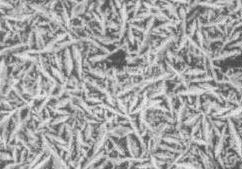
Graphitised carbon black is a stable and highly reproducible standard and is considered to be a standard resolution test for transmission electron microscopes. Mounted on a 3mm TEM grid.
These graphitised carbon black particles have lattice planes following the contours of the particles. For a good test of the instrument, choose a field of view where the lattice planes run in several different directions.
Lattice spacing 0.34nm.
Documents
Resolution, image quality, magnification and instrument stability in high performance TEMs can be checked by imaging the 0.204nm, 0.143nm and 0.104nm planar spacings in these specially prepared gold crystals. The tests are particularly recommended if height adjustments are made on the TEM specimen stage. The gold foil is mounted on a standard 3mm gold TEM grid.
The approximately 11nm thick evaporated gold is induced to grow in a (100) orientation. This gives lattice plane spacings of 0.204nm for the (200) planes and 0.143nm for the (220) planes. If the crystal thickness happens to be suitable, and if the objective aperture is large enough to accept the required diffraction beams, a spacing of 0.102nm can be imaged with a suitable focal setting. This specimen thus provides a valuable test for the best microscopes in service.
SEM
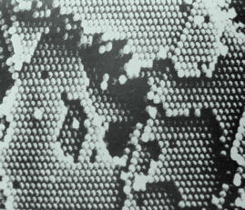
This specimen makes stigmatism in the obvious and the image is easily made astigmatic. Specify for mounted version.

SEM
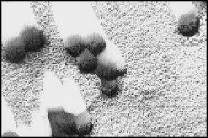
Islands of gold on a smooth carbon background. For testing high resolution and grey levels in with probe size below 10nm.Specify for mount.
S015H - Similar to the above but very small gold islands, < 2nm - 30nm, for ultra high resolution. Suitable for testing at magnifications of >50,000X. Specify for mount.
Documents
For TEM & STEM
These latex particles have a diameter of ~0.20µm (actual given with item), they are supported on a Formvar/ carbon film and shadowed with a coating of gold. Measuring the finest migrated gold particles in the shadow may be used to determine the resolution of the STEM or TEM. This test specimen is mounted on a 3.05mm copper grid.
Documents

For SEM, AFM & LM
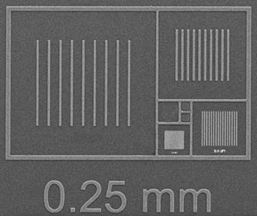
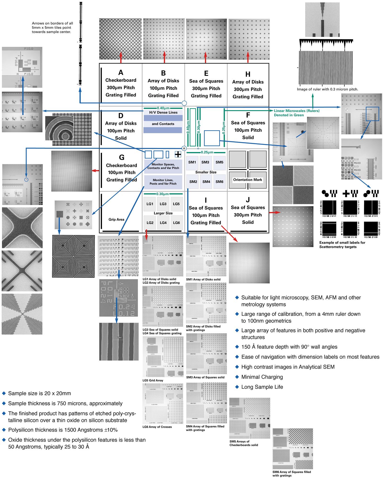
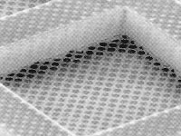
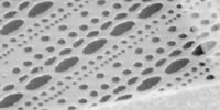
The MetroChip microscope calibration standard for SEM, AFM, light microscopy and metrology systems provides an extensive range of targets with periodic features for enhanced calibration down to the 100nm range. The MetroChip standard is produced with today's nanotechnology demands in mind. It is designed for a long life use and presents a stable calibration platform. The standard is on a 20 x 20mm chip with a thickness of 750µm. It delivers high contrast images for analytical SEM with minimal charging and combines a huge calibration range from 4mm down to 100nm.
Target calibration for SEM features include alignment marks, linear microscale, distortion measurements, par-axial calibration (image shift), resolution measurements, focus star, stigmator calibration, gratings, concentric circles and squares. The combination of these targets on one standard makes the MetroChip ideal as an all-in-one standard for setting up and regular calibration checks of the SEM or FESEM. For light microscopy and AFM, there are several targets to check linearity, distortion and scan length.
The sample can be used for calibration of several types of microscopes such as scanning electron microscopes, scanning ion microscopes, scanning probe microscopes (including AFM) and light optical microscopes in reflected mode.
Features
- Suitable for (reflected) light microscopy, SEM, AFM and other metrology systems
- Large range of calibration, from a 4mm ruler down to 100nm geometrics
- Large array of features in both positive and negative structures
- 150nm feature depth with 90° wall angles
- Ease of navigation with dimension labels on most features
- High contrast images in analytical SEM
- Minimal charging
- Long sample life
- Sample size is 20 x 20mm
- Sample thickness is 750 microns, approximately
- The finished product has patterns of etched poly-crystalline silicon over a thin oxide on silicon substrate
- Polysilicon thickness is 150nm ±10%
- Oxide thickness under the polysilicon features is less than 5nm, typically 2.5 to 3nm
The MetroChip calibration target is fully traceable to NIST certification.
View the example image in high quality (Right click > Open link in new tab)
Certification: Traceability of Sample Pitch
Report of Calibration NIST Test No. 821/271639-05
Documents

ProSciTech is proud to introduce the world's smallest ruler (5 micrometers) for the calibration of Transmission Electron Microscopes.
The MAG*I*CAL ™ has been developed to perform the three major calibrations of a TEM.
- Image Magnification Calibration.
- Camera Constant Calibration for Indexing Diffraction Patterns.
- Image/Diffraction Pattern Rotation Calibration.
With this newly developed single crystal material, a single sample can replace up to 5 other calibration samples.
The sample consists of an ion milled cross section of a silicon single crystal.This consists of a series of atomically flat layers of Si and SiGe which have been grown epitaxially by MBE(molecular beam epitaxy). The thickness' and spacing of these layers are very accurately known and all other spacings on the sample are easily verified. The layer spacings are designed so that the sample can be used to calibrate the entire magnification range in a TEM-from 1000X to 1,000,000X. And, since the material is a single crystal, it can also be used to perform the camera constant calibration and the image diffraction pattern rotation calibration.
The sample comes with simple, specific instructions for all calibrations.
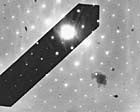
Figure 1. Diagram of the deluxe MAG*I*CAL™ calibration sample. The arrows indicate the four possible regions of interest on the sample where the calibration marks may be found. Note that this cross-sectional sample consist of two pieces of silicon wafer epoxied face-to-face, with additional silicon added as backing material to form a 3mm disk. To find the areas of interest at low magnification, look for the epoxy line on either side (between the arrows in the above figure).
Figure 2. TEM micrographs of the MAG*I*CAL™ calibration sample. The sample consists of a series of layers whose thickness are accurately known, based on the (111) lattice spacing of Si. Inset shows a higher magnification image of one of the layered structures.
ProSciTech stocks three types of QUANTIFOILS mounted on Cu/Rh grids. For other types and grid metals see previous item.


QUANTIFOIL® is a perforated support foil with pre-defined hole size, shape and arrangement. It has advantages in electron microscopy (EM) or low-energy electron point source (LEEPS) microscopy when compared with conventional holey film.
QUANTIFOIL® is offered with circular and square, orthogonal arranged holes. Films with different hole sizes and bar widths are available. Carbon is the standard material for the foil.
QUANTIFOIL® is a superior quality of holey carbon film, which facilitates the use of automation in TEM. (The Imaging Technology Group of Dr. Bridget Carrageen, University of Illinois at Urbana-Champaign, has developed a system called Legion, for automatically acquiring images from a transmission electron microscope)
QUANTIFOIL® with circular holes is used in cryo-electron tomographic reconstruction. The roundness of the holes is advantageous with respect to the formation of an ice layer of constant thickness. The hole size chosen depends on the magnification used, and on whether or not one wishes to include support film in the image. Assessment of the image quality is easier when foil is included in the picture, because the power spectrum of a foil is stronger than that of unsupported ice.
The surface properties of QUANTIFOIL® holey carbon support film, especially the wetting properties, may have to be adapted according to one’s particular requirements. Untreated aging QUANTIFOIL® tends to be hydrophobic. The foil can be made hydrophilic by glow discharging in residual air or by metal coating.
QUANTIFOIL® in low-energy electron point source (LEEPS) microscopy. QUANTIFOIL® with a regular pattern is required in order to be able to distinguish an object, which is spanned over a hole. An object cannot be discriminated from the support in the case of conventional holey support film. (H.W. Fink & C. Schonenberger, University of Basel, used QUANTIFOIL® for the measurement of electrical current through DNA molecules.)
The foil is ~12nm thick and mounted on copper or gold grids with either square or round holes of different sizes. If you require gold grids, please ask for a quote.
- QUANTIFOIL® R 1.2/1.3. A foil with ~1.2µm circular holes and a spacing of ~2.5µm between the holes. This type is used at magnifications around 50.000x.
- QUANTIFOIL® R 2/2. Holey films with 2µm circular holes are used at magnifications between 30.000x and 40.000x. R2/2 has 2µm holes and 4µm spaces.
- QUANTIFOIL® R 2/4 may be preferred over R 2/2, when an increased tolerance with respect to the position of beam, and a larger beam diameter are desired, such as in the case of automated image acquisition. R2/4 has 2µm holes and 6µm spaces.
- QUANTIFOIL® R 2/1 has more open area than R 2/2. It is used when focusing is carried out on the edge of a hole burnt in the ice in a neighbouring hole instead of on the foil adjacent to the hole. R2/1 has 2µm holes and 3µm spaces.
- QUANTIFOIL® with square holes and relatively narrow bars can be used in EM to support a thin carbon film, which by itself is too fragile to span a grid square. Alternatively, this holey film can directly support an object that is larger than the holes.
- QUANTIFOIL® S 7/2 constitutes an optimum between a maximum of open area on the one hand, and mechanical stability on the other hand. S7/2 has 7x7µm holes and 9µm spaces.
- QUANTIFOIL® Multi A is a holey film, which consists of various pattern hole sizes, shapes and arrangements. In addition to round holes, the pattern includes oval-shaped ones, which appear round at high tilt angles (~70°). The diameters of the round holes are about 1, 1.4 and 2µm, and the bar widths range from 0.5 to 4µm. The oval holes in the foil have a dimension of 8 x 2µm and 4 x 1µm.

TEM, SEM & LM
Polystyrene latex spheres have been used to calibrate electron microscopes since 1949 when a batch of uniform-sized particles was discovered by Backus and Williams at Dow Chemical. Since then, many graded sizes have been produced and these find a wide variety of applications in laboratories.
ProSciTech has increased the number of calibrated latex spheres available to twelve sizes; they range between 0.1 and 20µm. They are useful not only for TEM but also for SEM and light microscopy applications. Cost of latex spheres is now quite low, so there is no reason for any lab not to keep suitable calibration spheres at hand.
Latex particles are especially suited for calibrating SEM and TEM magnifications. If several particles are measured at a magnification where the particles are large enough to make an accurate measurement, it can be assumed that the average particle is within 1% of the nominal magnification. Latex particles are fairly inert and do not distort under vacuum or other normal operating conditions.
Latex particles are also used as an internal magnification standard and for estimating particle concentrations by combining equal size drops of latex particles and of a specimen solution.
It is possible to calculate the approximate number of latex particles in the supplied solution using below data or the link to the Spherotech information, which is applicable to any such latex spheres. However, greater precision in determining the particle numbers present is achievable if an electronic particle counter is used.
Adding a tiny amount of the working solution to the specimen surface makes accurate sizing and measurements possible. This is quite useful for all types of microscopy and especially so in SEM when the specimen is not flat and large size errors are possible because of perspective and varying working distances. It is also possible to make up a mixed size solution and this may be employed for comparative measurements of larger and smaller structures.
ADJUSTING PARTICLE NUMBERS TO REQUIRED CONCENTRATIONS
Usually the supplied concentration is too great and requires dilution with high purity water to make a working solution. In microscopy for a given application the number of particles used, regardless of size, needs to be fairly uniform. The number of particles in a given weight/volume solution varies dramatically with particle size. These numbers are given in column two (in the table below) and relate to a 0.1% solution. For a 1% solution its simply x10 and for a 5% solution x50. Column three gives the dilution required to achieve 3.6x10e-6 particles /mL for various latex particle sizes.
| Diameter (µm) | Number of particles/mL | 3.6x10e-6/mL |
| 0.1µm | 1818 x 10e9 | ~3.6 x 10e-6 % |
| 0.5µm | 14.5 x 10e9 | ~4.6 x 10e-4 % |
| 1.0µm | 1.8 x 10e9 | ~3.7 x 10e-3 % |
| 0.3µm | 67 x 10e9 | ~1 x 10e-4 % |
| 3.0µm | 67 x 10e6 | 0.1 % |
| 5.0µm | 14,5 x 10e6 | ~0.46% |
| 10µm | 1.8 x 10e6 | ~3.6% |
| 15µm | 0.5 x 10e6 | ~12.4% |
Particle concentration of latex calibration spheres for microscopy are supplied as 0.1% weight by volume within an aqueous solution. Specific gravity of spheres is 1.05. The solution contains an antibacterial agent.
Twelve different particle sizes are available. Each tube of the "small" and "medium" sizes contains 5mL. Larger spheres are more expensive and different volumes are used for these. Lids are colour coded contamination between different sizes. Sizes are nominal and the actual size is indicated on the vial.
For a large range of SPHEROTECH special application latex particles see page Q1
LATEX SPHERES FOR MICROSCOPY
Available in the following sizes.